- 13240518155
- sales@vision-pcb.com

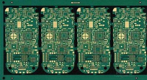
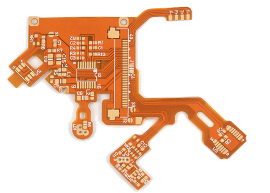
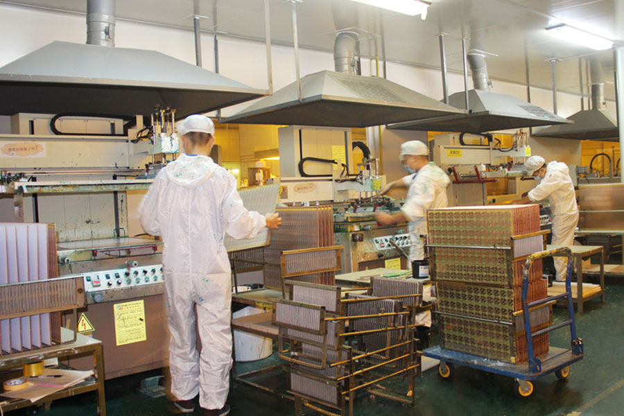
Vision Pcb Indusry Co.,Ltd. was founded in June 2004.The company mainly produces templets and quick components, which specializes in manufacturing highly sophisticated and high PCB boards including single-layer, double-layer, multi-layer boards, MID, HDI, impedance boards, aluminum-backed boards, mixed platens and various special boards, various flexible PCB and rigid-flex PCB. The company establishes production base with super-size, with more than 500employees, and daily delivery ability reaches types, and monthly delivery ability reaches types. Address of the factory: Lantian technology park, Sha’er village, Shajing street, Shenzhen, which is adjacent to main electronic industrial cities, with convenient transportation and quick services.
Company feature:provide all-around solutions for the customers, and solve the urgent problems for the customers, and our company provides -hour emergent single and double boards and emergent business for four-layer boards, and we can guarantee quick (quick delivery speed), good (good product quality), economic (low procurement cost) and exceeding customer’s alternatives).
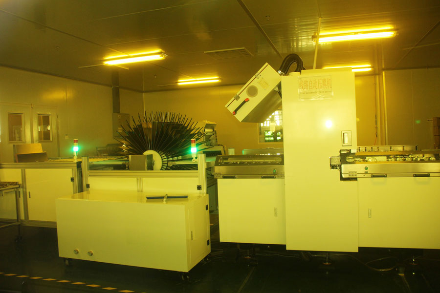
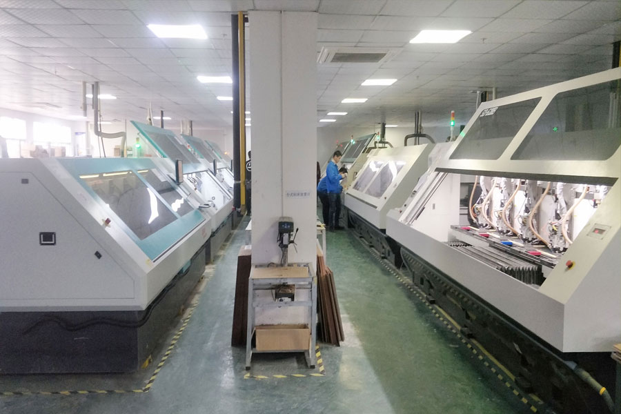
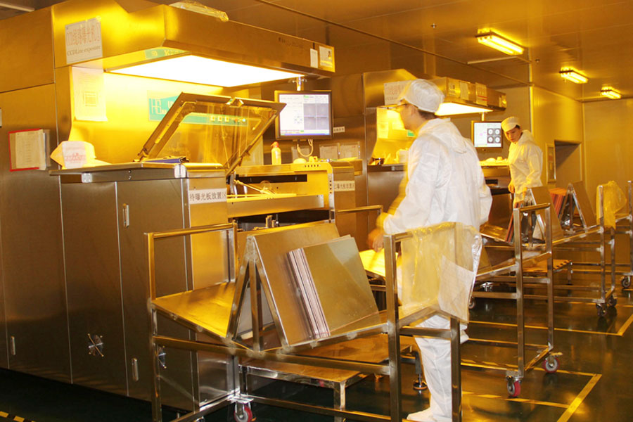
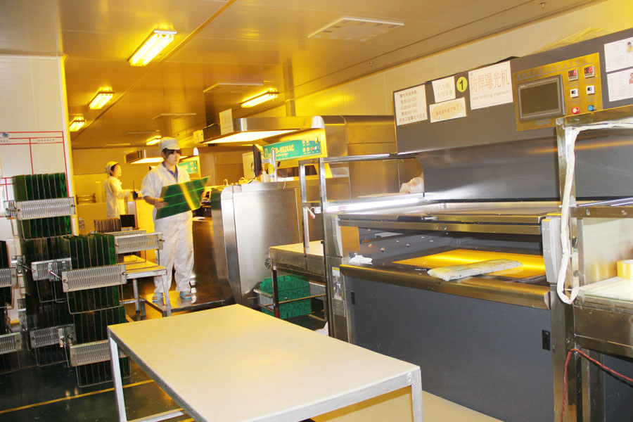
Quality assurance:our company hasss leading flying probe testing technology in the industry, and purchases advanced production and testing equipments from US, Japan, Germany and Israel etc, which improve the manufacture of various high difficulty boards including buried blind hole boards and flat computers. .
Applicable range of the product: the company’s products are extensively applied into electronic fields in healthcare, flat computer, communication, auto, power, security, industrial control, telecommunication, remote control and consumption etc.
Operational and management tenet:the company’s size is big, which is circuit board production enterprise with the sophisticated equipments, strict management and brilliant quality. The company inherits standards, and adheres to perseverance, and all the employees are involved into quality improvement, and continuously absorbs international latest technologies, and completes product quality and satisfies customer’s needs.
Vision pcb manfacture high qualtiy pcb for thousands of customers from all over of the world
One of the lowest price suppliers in China
Quikest Turn 12 hours for sample pcb
Quote with in one hour,24hours service
One-stop servcie from pcb copy-design- components sourcing- stencil fabrication-pcb fabrication- assembly- packing-- shipment
Call 13240518155
Common Pin Names and Functions in Power ICs: Understanding Special Pins in DC-DC ChipsIn addition to the regular input and output pins, common DC-DC chips also have some special pins. What are the full names of these pins and what are their functions? To help everyone quickly identify chip functions, this article will introduce the common pin names in power ICs.01 RT/CLK/SYNCRT is the internal oscillator frequency control pin of the DC-DC, where R stands for resistor. Generally, a resistor is connected to the ground to control the working frequency of the DC-DC. The resistance value is usually provided in the form of a table in the datasheet.SYNC and CLK are external clock input pins for the DC-DC. SYNC stands for synchronizing, and CLK stands for clock. These pins connect to an external clock source to control the operating frequency of the DC-DC. The advantage of external clock input is that when there are multiple DC-DCs, using the same clock can reduce the total input current ripple, which is beneficial for the EMC of the circuit.RT and CLK may sometimes be the same pin.02 PG/PERGD/PGOODThe power status indicator pin, which is generally an open-drain output, requires a pull-up resistor. This pin can be connected to an LED indicator light or an MCU IO. It outputs a high level when the power output is normal and a low level when the power output is abnormal.03 FB/VSENSEThe FB pin is the feedback pin. Once negative feedback is formed, it fixes the voltage. The voltage value is provided in the datasheet. For example, in the figure below, the FB voltage Vfb is known to be 0.6V, so the output voltage = Vfb * (1 + R1/R2).04 COMPThis pin is the output of the error amplifier and the input of the PWM comparator. It is generally connected in series with a capacitor and resistor for frequency compensation. Depending on the principle, it may be connected to ground or the FB pin. Why is frequency compensation necessary? During the operation of the power IC, the load may suddenly increase or decrease, requiring high dynamic performance from the power IC to avoid voltage drops or overshoots. If the output voltage is unstable during load changes, the capacitance and resistance connected to the COMP pin should be adjusted.05 BOOT/VBSTThe BOOT pin is the boost capacitor pin for the high-side FET gate driver. This pin is generally connected to a 0.1uF capacitor to the SW pin to increase the gate drive voltage.As shown in the figure, to turn on the high-side NMOS, the gate voltage G of the NMOS should be higher than the source voltage SW. However, when the SW voltage is close to the input voltage VIN, VG cannot be higher than the SW voltage. Therefore, the VBST capacitor is needed, using the characteristic that the capacitor voltage cannot突变, to increase the supply voltage of the HS operational amplifier to be greater than the SW voltage, i.e., greater than the input voltage VIN, so that the G voltage is greater than SW.06 CS/CSGC stands for Current, S stands for Sensor, and G stands for GND. Generally, a shunt resistor is connected between CS and CSG to read the current. ICs with adjustable current limiting protection usually have these two pins.07 EN/ON#OFFEN is short for Enable Pin, which means the enable pin. It requires a certain voltage or grounding to control the switch of the IC. In most applications, it is enabled by connecting a resistor to the input pin.08 EP/PADEP stands for Exposed Thermal PAD, which is the exposed thermal pad of the package. It should be connected to ground to facilitate heat dissipation.09 SW/PHThe SW pin is generally connected to the inductor because this pin is also connected to the MOSFET switch inside the DC-DC, so SW is short for Switch.10 Reference ICs are as follows:TI: LM5118, TPS54331, TPS54360B, TPS56320x, TPS54231, TLV62569, TPS51200, TLV62130x, TPS54240, etc
Details
Hello everyone, today we will delve into a crucial aspect of electronics manufacturing - PCB panelization design. This is not just a technical task but also a vital means of improving PCB manufacturing efficiency and reducing PCB cost.Why is PCB Panelization Necessary?After the completion of PCB design, we face the production processes of board making and component placement. Producing individual cards separately not only wastes material but also affects production efficiency. Therefore, panelization design has become a key step in enhancing production efficiency and cost savings.Cost Savings in Production: Rational panelization can save on board material and reduce waste area, thereby lowering production costs.
Details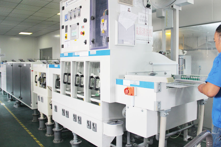
Designing 10-layer or multilayer PCBs presents significant manufacturing challenges compared to conventional circuit board products. High-layer boards are characterized by a thicker board, more layers, denser circuits and vias, larger unit dimensions, and thinner dielectric layers. The requirements for inner layer space, interlayer alignment, impedance control, and reliability are more stringent.I. Interlayer Alignment ChallengesDue to the multiple layers in high-layer boards, customers have increasingly strict requirements for interlayer alignment, typically controlled within ±75μm. Factors such as the larger unit size design of high-layer boards, environmental temperature and humidity in the graphic transfer workshop, and the inconsistency in expansion and contraction of different core board layers contribute to the increased difficulty in controlling interlayer alignment.II. Inner Layer Fabrication ChallengesHigh-layer boards use special materials such as high-TG, high-speed, high-frequency, thick copper, and thin dielectric layers, which pose high demands on the fabrication of inner layers and control of graphic dimensions. This includes the integrity of impedance signal transmission, increasing the difficulty of inner layer fabrication. Small line widths and spacings lead to an increase in open and short circuits, micro shorts, and low yield rates. The probability of AOI inspection missing defects in dense signal layers is higher. Thin inner core board thickness is prone to wrinkles, leading to poor exposure and rolling during etching. Most high-layer boards are system boards with larger unit sizes, resulting in a higher cost of scrap.III. Lamination ChallengesWhen multiple inner core boards and prepreg sheets are stacked, lamination production can easily lead to defects such as panel shift, delamination, resin voids, and bubble residue. In the design of the lamination structure, it is necessary to fully consider the thermal resistance, voltage resistance, filling amount of materials, and dielectric thickness, and set a reasonable lamination program for high-layer boards. The control and dimensional compensation of expansion and contraction cannot be consistent due to the multiple layers; the thin interlayer insulation layer can easily lead to interlayer reliability test failure issues.IV. Drilling ChallengesThe use of special materials such as high-TG, high-speed, high-frequency, and thick copper boards increases the difficulty of hole roughness, burrs, and debur. With multiple layers, the cumulative total copper thickness and board thickness lead to easy breakage of drill bits; dense BGA leads to CAF failure issues due to narrow hole wall spacing; and board thickness easily leads to drilling inclination issues.
Details